 |
| Photo Transistor |
In this topic we we learn the
construction and working of a photo-transistor and an opto-coupler. These are
related components hence will cover in same post. As we saw about photo diodes
in previous topic, a photo-transistor is similar to a normal transistor in
construction with a difference that the photo transistor can be operated by applying
light on base-emitter junction rather than providing base current to drive the
collector current. Mainly it is operated by light radiation on junction but
optionally it can be operated as normal transistor if the base pin is provided
for external connection. Base terminal may not be provided in some of the photo
transistor models.
Construction:
As we can see in the diagram showing a
N-P-N photo transistor having N-P-N junction as a regular transistor. The main
difference is that the outer packaging of such transistor will have transparent
window or lens to allow light to fall on the Base-Emitter junction to activate
the transistor. Light photons activate the transistor and the base current
increases exponentially as the light flux falling on it is increased. These
transistors respond to visible light as well as Infrared light. This way photo
transistor act as light sensor as it can change light energy into electrical
energy, similar to Photo Diodes and Light Dependent Resistors (LDR). The only
difference is that LDR and Photo Diodes are passive component, that means they
do not do any type of amplification of electrical energy as compared to photo
transistor which is an active semiconductor device.
 |
| Symbol |
They come in both types i.e. N-P-N and
P-N-P, based on the materials used in construction. Symbol of both types are as
shown here. It is similar to normal N-P-N and P-N-P transistor with two arrows
pointing towards base terminal showing they are light activated. Similar to
normal transistor symbol, direction of arrow in emitter indicates the direction
of flow of current when used in a circuit.
 |
| Photo Transistor Circuit |
The diagram shows here how we can use a
photo-transistor in a circuit. Load RL is connected again to the collector
of the transistor. Now instead of providing any electrical connection to the
base of the transistor, we are allowing light to fall on transistor which will
activate the transistor and current will start flowing through the load resistor
connected at collector. We will see how such photo transistors are used in a
opto-coupler to electrically isolate two circuits from each other.
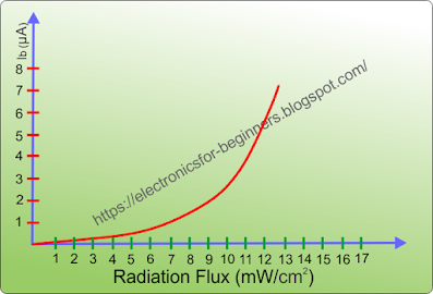
The graph shown here indicates the
increase in base current due to increase in light energy falling on
base-emitter junction of photo transistor. It shows exponential increase in
base current due to increase in light intensity, but after certain level of
light the transistor will reach saturation as all available current carriers
would be in motion and there are no more current carriers left to be activated
by more light.
Opto-coupler:
 |
| Sample Opto-Coupler |
As the name denotes, these are
components which couples two circuits optically i.e. they allow two circuit
parts to be connected to each other via light rather than any electrical
connection between them. Opto-couplers comes in 4-pin or 6-pin IC packages
(Integrated Circuits). We will learn in detail about IC in later topics. As of
now we should know that IC packages are small rectangular components packed
with a small circuit inside it hence named as “Integrated Circuit”, a circuit
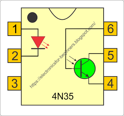
integrated inside a package. Here we see a photo transistor inside the
rectangular box with base terminal internally connected to pin#6, emitter to
pin#4 and collector to pin#5. On the left hand we have a LED connected to pin#1
& 2 and pin#3 is unused. This is one type of opto-coupler which is using photo
transistor, there are other opto-couplers which uses some power semiconductors
which we will see at later stage.
 |
| Opto-Coupler Circuit |
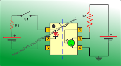
Now let us see this connection diagram
showing an opto-coupler connected in a circuit. The LED pins on left side is
connected to a cell using a resistor ‘R1’ to limit the current in LED, which is
fed to it through a switch ‘S1’.
On the other hand a load (R2) is
connected on collector of transistor (pin#5) to the positive of right side cell
and emitter is connected to its negative terminal. Load can be any thing which
the transistor can drive, like relay, small DC light etc. Since we are
operating the opto-coupler through light of LED, we do not need to connect pin#6
(base of transistor).
When the switch S1 is in off position,
the LED is in off condition and hence the photo transistor is also in cut of
mode hence no current flows in the resistor ‘R2’.
If we turn ON switch ‘S1’, the light
coming out from LED falls on the photo transistor hence it start conducting
and current start flowing from load resistor ‘R2’.
Now if we draw a partitioning line
in the middle as shown with blue dotted line, we can see there are two small
circuits, one at left and other on right which are electrically isolated from
each other as there is no wired connection between both circuits. They are
still connected to each other only through the light generated by the
LED, hence called an Opto-coupler.
This type of circuit is mostly used
when we have low voltage and delicate circuit driving high voltage circuits. Example
when a micro-controller/microprocessor is controlling some high voltage
circuit. We will learn about micro-controllers and microprocessors when we will
complete basics of digital circuits. Any small fluctuation in electrical current in high voltage circuit may cause
damage to low voltage operated micro-controller, hence these opto-couplers play an
important role there.
That’s all about opto-couplers, next we
will learn about analogue and digital signals and will slowly move on to
digital number system and digital gates.


0 Comments